
- Company overview The heart of SMC Vision & Philsophy Partnership Certifications Company culture
- Our service Design and Engineering Maintenance and Service Examine Production Line Upgrade and Transformation Storage and Logistics Processing, Trading and Distributor
- Management Our history Global responsibility Info Center
- Procurement center Internship
- Construction & Real Estate
- General Mechanical Equipment Refrigeration Equipment Metal & Metallurgy Machinery Other Equipments Compressor
- Safety Roadway Safety Personal Protective Equipment
- Mechanical Basic Parts Bearing Spare Parts
- Hardware Tools
- Instrumentation Testing and Analysis Instruments Other Instrumentations
- Electrical & Electronics
- Construction Machinery Lifting Machinery Earth Moving machinery Road Construction Machinery Drilling Machinery Logistics Machinery Generator Set & Engine Other Machinery
- Rubber & Plastics Plastic Pipes and Pipe Fittings Fiberglass Reinforced Plastic Pontoon System PCTFE Product Polymer Material
- Industrial Gas Container
- Hotel Equipment & Supplies
- Daily Necessities Fabric Products Glasswork Pet Supplies
- Environmental Protection Machinery
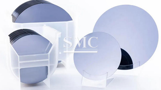
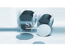
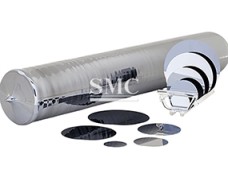
Monocrystalline Silicon Wafer


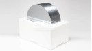
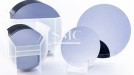

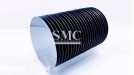

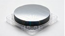

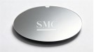

Material: Single Crystal Silicon (CZ / FZ grown)
Diameter Range: 2″ – 12″ (50.8 – 300 mm)
Thickness: 100 – 1000 µm (±10 µm)
Crystal Orientation: (100) / (111) / (110), ±0.5°
Surface Finish: Polished / Lapped / As-cut / Epi-ready
Shanghai Mac Corporation is a leading Monocrystalline Silicon Wafer manufacturer and supplier.
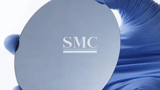
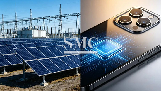
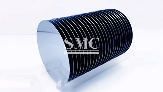
A monocrystalline silicon wafer is a thin, disc-shaped slice cut from a single crystal silicon ingot grown by the Czochralski (CZ) or Float Zone (FZ) method. It is the fundamental substrate used to build integrated circuits (ICs), discrete power devices, MEMS sensors and photovoltaic solar cells, because its continuous, defect-controlled crystal lattice delivers predictable electrical and mechanical properties that polycrystalline silicon cannot offer. By supplying wafers with precisely controlled diameter, thickness, resistivity, flatness and surface finish, we help chipmakers and module manufacturers cut process variation, raise device yield and lower unit production cost. Our wafers range from 50.8 mm to 300 mm in diameter, in (100), (111) or (110) orientation, P or N type doping, with resistivity from 0.001 to 10,000 Ω·cm, covering both R&D prototyping and high-volume production lines.
If you want to know more about our Monocrystalline Silicon Wafer or product price, please feel free to contact us, we will reply you within 24 hours.





Crystal & Electrical Parameters
1. Parameter SGrowth Method: CZ (Czochralski) / MCZ / FZ (Float Zone)
2. Oxygen Content (CZ): 10 – 18 ppma
3. Carbon Content: ≤ 1 ppma
4. Dopant Concentration: Per customer specification
Wafer Manufacturing Process
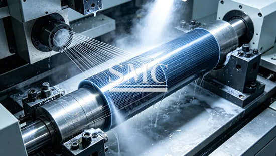
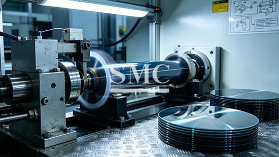
Polysilicon feedstock → Crystal growth (CZ / FZ) → Ingot grinding & orientation → Wire saw slicing → Edge rounding → Lapping / grinding → Wet etching → Mirror polishing → Precision cleaning → Optical inspection & packaging.

Standard Packaging
Each wafer is sealed in a nitrogen-protected vacuum aluminum foil bag with anti-static protection, then placed individually into a clean plastic wafer cassette or rigid wafer shipping box. Cassettes are packed in reinforced export cartons together with moisture-absorbing desiccant and ESD warning labels, and the cartons are stacked on fumigated wooden pallets wrapped with stretch film for international shipment.
Shipping
We support FCL and LCL sea freight, air freight and express delivery depending on order quantity and destination. Common trade terms include EXW / FCA / FOB / CFR / CIF; other terms may be available upon request.
Shipping costs are calculated based on cargo volume, gross weight, destination and selected transportation method. Packing list, commercial invoice and certificate of origin can be provided with each shipment.
Lead time
Samples: 3 – 7 working days
Standard orders: 15 – 25 working days
Customized orders: 25 – 40 working days


Q: How long does sample preparation take?
A: Standard samples are ready within 3–7 working days after specification confirmation, and are shipped by express together with the full inspection report (resistivity, TTV, bow/warp and surface particles).
Q: What information do you need for a custom quotation?
A: Please provide diameter, thickness, crystal orientation, conductivity type (P/N), resistivity range, surface finish, grade (prime/test/dummy) and quantity. We will respond with a quotation within 24 hours.
Q: What is the MOQ and production lead time?
A: The MOQ is 25 wafers for standard polished wafers. Standard orders ship in 15–25 working days and customized orders in 25–40 working days, depending on size and grade.
Q: What quality standards does the product meet?
A: Wafers are produced and inspected according to SEMI M1 and SEMI M59 (and SEMI PV22 for solar grade), with a certificate of analysis covering electrical, dimensional and surface parameters for each batch.
Q: What is the difference between CZ and FZ silicon wafers?
A: CZ (Czochralski) wafers are grown from a melt in a quartz crucible, offering large diameters (up to 300 mm) at lower cost but with higher oxygen content. FZ (Float Zone) wafers are grown without a crucible, giving much lower oxygen content and higher resistivity — preferred for high-voltage power devices such as IGBT.
Q: What is the difference between polished, lapped and as-cut wafers?
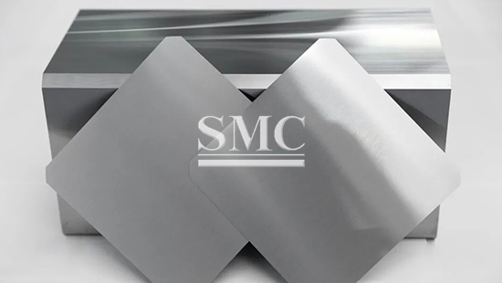
A: As-cut wafers come directly from wire sawing and still carry saw marks; lapped wafers have a flat, uniformly ground surface; polished wafers have a mirror-smooth, particle-free front side ready for epitaxy and lithography. As-cut suits solar cells, while polished suits IC and MEMS fabrication.
Q: How do I choose the right wafer orientation for my device?
A: (100) is dominant for CMOS logic and memory because it cleaves easily and gives good gate oxide quality; (111) is used for bipolar and power devices; (110) is used for special MEMS structures. Tell us your device type and we will recommend the best orientation.
here
for
price